


The Secret Behind TSMC’s CoWoS Packaging Technology
The long-awaited big break in 3D IC packaging has been years in the making. Since its debut at SEMICON Taiwan over a decade ago, TSMC’s CoWoS 3D packaging business has grown 60% every year. What made TSMC buck the odds?
Source: here
SEMICON Taiwan 2024 is this year’s iteration of the annual extravaganza for the global semiconductor industry.
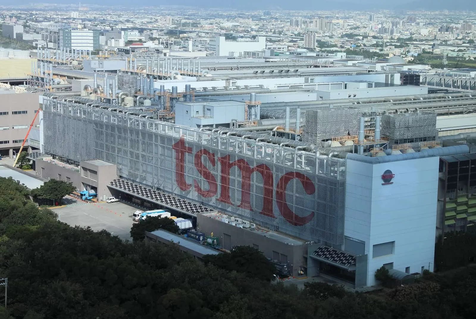
TSMC’s CoWoS integrated circuit packaging technology, which was a revolutionary breakthrough in semiconductor manufacturing, debuted at SEMICON 13 years ago.
At the time, all that anyone in the field could talk about was “3D IC”. The idea was to package multiple dies side-by-side on the silicon interposer at a wafer level to greatly enhance interconnect density and reduce chip footprint. Other industry giants like the ASE Group and Siliconware Precision Industries Co. (SPIL) were champing at the bit to get in on the ground floor.
But then, a senior director from TSMC dropped a bombshell during the forum: TSMC was getting into the 3D IC business, offering a simplified version of the advanced packaging technology to its clients.
IC packaging companies were in agony. “Are you saying that we’re out of a job?” The vice president of research and development at a major company asked in distress.
During TSMC’s shareholders’ meeting a month later, Morris Chang (張忠謀) officially announced that TSMC was introducing its CoWoS “chip-on-wafer-on-substrate” technology.
Rumor had it that the backlash from the packaging industry was so fierce, Chang had to make a personal announcement to soothe the controversy and make it clear that he stood behind his company’s decision.
The senior director who started the whole affair was none other than Dr. Douglas Yu (余振華), Vice President of Pathfinding for System Integration at TSMC, who has recently been awarded a fellowship at Academia Sinica. He was the pioneer behind two of TSMC’s most groundbreaking technologies: CoWoS, which is used in high-performance computing, and InFO, which is used on mobile devices. The former is the darling of Nvidia’s GPUs; the latter is used in Apple’s self-developed computer chips. This was a whole new wellspring of revenue for TSMC.
In his announcement, Chang declared that the reason that TSMC was getting into the packaging business was to create “a clear ownership of [the] long process flow.”.
This reporter did not quite understand the explanation until years later. At its core, the question boils down to “who should pay—and how much should they pay—when something breaks?”
Take Nvidia’s AI accelerator, the H100 GPU, as an example. If its architecture was a slice of Hawaiian pizza, the ham on top would be the 4-nanometer GPU chips, and the pineapple pieces would be High Bandwidth Memory (HBM). The cheese below would be the silicon interposer, which rests atop the dough—the IC substrate.
When packaging companies talk about working with 3D IC, think of it as TSMC making the “ham” and selling it to ASE or SPIL, who would then buy the “pineapple” from SK Hynix Semiconductor to combine everything into a slice of pizza.
A packaged H100 chip costs over US$30,000. Just the “ham” made by TSMC costs a few thousand dollars.
Packaging companies face a harsh reality. The “cheese” in the middle, the silicon interposer, requires wafer-level manufacturing expertise. It is extremely difficult. Failure would mean that the expensive “ham” on top would be kaput as well.
Herein lies the point of contention. TSMC’s profit margin is over 50%, which means its “ham” has a price tag that is double the cost. But if TSMC did the packaging itself, the cost of failure would not include the lucrative profit margin.
“If they broke it, they bought it. But if I broke it, I’d have to pay twice as much. Of course it’s hard to compete,” Mike Ma (馬光華), the former vice president of research and development at SPIL who single-handedly built its advanced manufacturing line, explained the dilemma to this reporter some years ago. Even if packaging companies quoted the lowest price possible, they still couldn’t compete. Ultimately, this led to TSMC monopolizing the field of advanced IC packaging.
New Hope for IC Packaging
The big break in 3D IC, which the packaging segment of the semiconductor supply chain has waited for all these years, is finally on the cusp of realization, thanks to generative AI. The manufacturing of the H100 chips has been limited by the production capacity of CoWoS. TSMC has agreed to give some of its orders to ASE and the American company Amkor Technology. However, this is restricted to the latter half of the CoWoS process. In other words, it’s the final phase when all the toppings are placed on the “dough”, or the IC substrate.
Industry veterans point out that TSMC has already accrued over a decade of mass production experience. “They are taking it easy because they are so far ahead.” But they also stipulate that contactors replicate TSMC’s process with zero variation, down to the equipment, materials, and production parameters.
The substantially more challenging first half of the process, “chip-on-wafer”, may also be outsourced to suppliers. ASE is gearing up for this once-in-a-lifetime opportunity. This is why its expenditure this year is a record-shattering US$3 billion.
TSMC Chairman Dr. C.C. Wei (魏哲家) introduced a strategy in July that he dubbed “Foundry 2.0”. The plan: expand the definition of wafer foundry to officially encompass packaging and testing. He feels that this new definition will offer a new shot at growth for TSMC.
How big of a chance is it? For CoWoS, TSMC is projecting a CAGR of up to 60% between 2022 and 2026. Advanced packaging is just 10% of TSMC’s business. In a few years, it could overtake ASE to become the world’s largest IC packaging company.
During the 2024 Technology Symposium, TSMC unveiled a new iteration of CoWoS called “system-on-wafer”, or SoW. It can produce a massive chip that’s about the size of a 12-inch wafer. These products will be used in a new generation of data centers.
It shows just how far TSMC’s technological dominance has come. In the past, chips were in a race to downsize. But due to demand from customers in the AI industry like Nvidia, a paradigm shift has occurred where the packaging process will churn out larger chips.
Wei has admitted that TSMC is also branching out into panel-level packaging, where chip size is even less of a limitation. At the earliest, the new products will launch in three years. We wouldn’t be surprised if Nvidia CEO Jensen Huang (黃仁勳) wows the crowd with new AI chips the size of desktops.
Have you read?