


Is China Catching Up in Semiconductor Talent? And Nvidia’s GPU Delay? Blame It on Heat and Expansion
Liang-rong Chen
Hello everyone,
Next week, July 9, will mark the showdown over reciprocal tariffs. In Taiwan, we’re seeing a stark contrast between two sectors: the struggling traditional industries, which stand to suffer the most, and the red-hot AI stocks. It’s a tale of fire and ice.
Interestingly, I recently noticed a similarly dramatic contrast playing out in Japan.
According to Nikkei, a group of nine Japanese entertainment companies, including Sony, Nintendo, Bandai Namco, Konami, Square Enix, Capcom, Nexon, Sanrio, and Toho, has seen their combined market capitalization surge by 28% so far this year, reaching $397 billion as of June 30. For the first time in 14 years, that total has surpassed the combined market cap of Japan’s top nine automakers, including Toyota and Honda.
Meanwhile, those nine automakers have seen their total market value drop 18% year-to-date. The outlook isn’t rosy either: Toyota and Honda are expected to see their profits for fiscal 2026 (ending March next year) fall by 30% and 60%, respectively. The main culprits? U.S. tariffs and intensifying EV competition, especially in China.
Toyota, long a symbol of “Made in Japan,” remains highly profitable, posting ¥4.76 trillion in net income for fiscal 2024—comparable to TSMC. Yet market sentiment remains bleak: its P/E ratio is just 6.9, about one-third of TSMC’s.
As someone who grew up on Japanese anime and video games like Street Fighter (Capcom) and Romance of the Three Kingdoms (Bandai Namco), it’s fascinating to see Western and emerging markets now catching the same wave of “Japanophilia” that once swept Taiwan.
Demon Slayer (Sony) has become a global hit on Netflix. Toho, the studio behind the Godzilla franchise, is enjoying a major revival thanks to box office success, with a P/E ratio of 31. Sanrio sits at 39, and Nintendo—buoyed by anticipation for the upcoming Switch 2—has reached a sky-high 53, even surpassing Nvidia’s 51.
This trend—booming cultural exports, declining manufacturing—is partly thanks to the content industry being tariff-free. But it also reflects the waning global competitiveness of Japanese manufacturing.
A venture capitalist active in Japan recently told me this divergence is “not a good sign” for the Japanese economy as a whole.
For reference, the combined market cap of those 18 Japanese companies still doesn’t match that of a single TSMC.
And TSMC appears poised for even more momentum, because its competitor just fell further behind.
Yesterday, Reuters reported exclusively that Intel’s new CEO, Lip-Bu Tan (陳立武), has decided that its newly ramped-up 18A process will no longer be offered to foundry customers, and will instead be reserved solely for Intel’s own products. This move effectively wipes out what could have become $1 billion in potential bad debt.
In other words, the grand 18A foundry push envisioned by former CEO Pat Gelsinger—meant to challenge TSMC—has, as many in the industry predicted, ended in vain. TSMC’s 2nm node is now essentially a solo act.
According to Reuters, Lip-Bu Tan is reallocating resources to the next-generation 14A process, aiming directly at TSMC’s two largest clients: Apple and Nvidia.
One has to wonder: is this just an excuse? Could Lip-Bu Tan be quietly stepping away from the foundry business altogether?
A senior executive at a major Taiwanese IC company who knows Lip-Bu Tan personally told me that doesn’t seem to be the case. He explained that Intel’s foundry ecosystem still needs time to mature, and for now, Lip-Bu Tan has no choice but to focus resources where they matter most.
One foreign analyst put it even more bluntly: “18A can’t be saved. The only option now is to go all in on 14A.”
Back to this week’s newsletter.
First, an apology: the original article planned for this issue has been postponed due to legal concerns, so publication was delayed by a day.
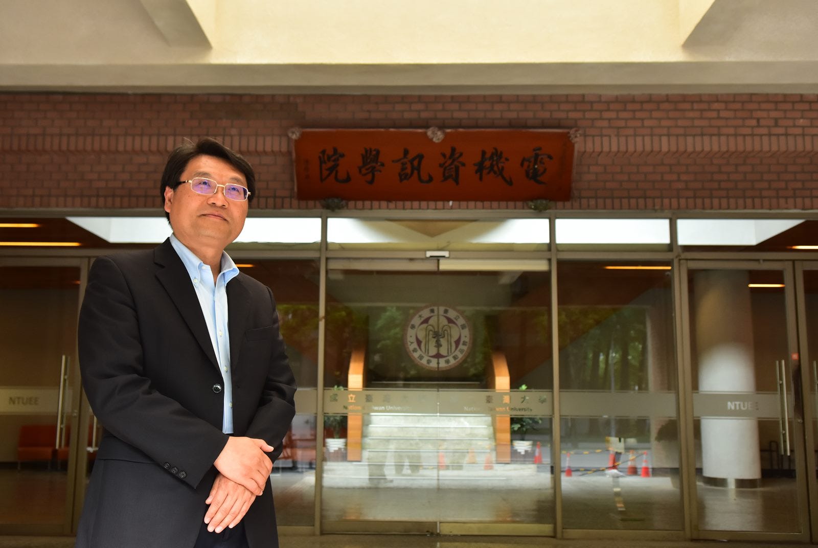
In its place, we’re running this podcast transcript featuring Professor Yao-Wen Chang(張耀文), a Distinguished Professor of Electrical Engineering at National Taiwan University. Many thanks to my colleague Mini Wu(吳廷勻) for the excellent write-up.
Professor Chang, who just stepped down as Dean of NTU’s College of Electrical Engineering and Computer Science, holds a prominent position in the global EDA academic community.
At the same time, his research is deeply attuned to industry needs. That’s why MediaTek(聯發科) Chairman Ming-Kai Tsai (蔡明介) invited him to join the company’s board as an independent director.
Recently, his team’s research has focused on solving some of the toughest challenges in today’s hottest field: advanced packaging, especially CoWoS.
Want to know why Nvidia’s GB200 is struggling to reach mass production? Or whether Taiwan’s semiconductor talent might be overtaken by China?
Check out this week’s newsletter.
How much damage will Trump’s proposed reciprocal tariffs actually do to Taiwan’s electronics industry? That’s still up in the air. What’s more concrete, and already here, is AI’s impact on IC design.
Take Nvidia’s(輝達) Blackwell-series GPUs. Over the past few months, mass production has been repeatedly delayed. The root cause? A major bottleneck in the CoWoS advanced packaging technology: warpage.
The problem isn’t hard to understand. These massive AI chips are assembled through ever-more-aggressive integration, combining components made with different processes and materials. But those materials all expand and contract differently when exposed to heat. It leads to mechanical stress, and sometimes, structural failure.
Ironically, the newest frontier of cutting-edge semiconductor technology is now being held back by one of the oldest challenges in physics: thermal expansion. It sounds like a solvable problem. So why has it proven so stubborn? Why, after five years, is this issue still unresolved, with trillions of dollars in investment effectively stuck on pause?
Dr. Yao-Wen Chang, a Lifetime Distinguished Professor of Electrical Engineering at National Taiwan University and an independent director at MediaTek, is a global authority in Electronic Design Automation (EDA). His current research focuses on solving these very issues using AI, while also analyzing the impact of AI hardware on the EDA industry.
AI is transforming every industry, and when we talk about “AI for EDA,” we also need to look at the reverse: how EDA is enabling the design of AI hardware.
Today’s AI models rely on massive GPUs, built using advanced packaging technologies that tightly integrate diverse components. But that complexity comes at a cost. After fabrication, these densely packed chips often suffer from warpage.
What causes warpage? It stems from mismatches in the coefficients of thermal expansion (CTE) between different materials.
In advanced packaging, a single system often integrates numerous chips. When the chips and the substrate have different CTEs, the repeated heating and cooling cycles during manufacturing lead to uneven thermal expansion and contraction. This mismatch can result in delamination, deformation, or physical distortion, causing the package to warp or bow.
Rising Complexity, Rising Heat
Why is it such a headache now? Advanced packaging requires extremely high precision. More fundamentally, the semiconductor industry has traditionally been dominated by engineers with electrical engineering backgrounds. But with advanced packaging, integrating a wide range of components from different domains introduces tremendous complexity.
Imagine packing numerous components into a tiny packaging system. It’s like squeezing 100 students into a classroom designed for 10. Naturally, the temperature rises. It’s a vivid metaphor for the thermal challenges plaguing today’s chips.
There’s also the issue of mechanical effects. Warpage itself is a manifestation of mechanical stress. And then there’s optics. Last year, TSMC began integrating silicon photonics — optical components — into its packaging systems. Since light is more energy-efficient and transmits faster than electricity, combining optical and electrical elements can significantly reduce power consumption.
TSMC demonstrated a package that consumed 2,400 watts using only electrical signaling, but with photonic integration, the same system could be brought down to just 850 watts.
Taiwan has been working on packaging technologies for over 20 years. Today’s major technology drivers, such as AI, high-performance computing, autonomous vehicles, big data analytics, and smart healthcare, all depend heavily on computing power.
Throughout this evolution, the semiconductor industry’s consistent pursuit has been to achieve faster performance, lower power consumption, and reduced cost. This is the essence of PPA optimization: performance, power, and area.
There are three major pathways to achieving this goal. The first is traditional process scaling, More Moore, pushing Moore’s Law forward. But with the advent of EUV lithography, the cost of continued miniaturization has skyrocketed.
The second, increasingly important direction is advanced heterogeneous integration. Even if some components are manufactured using mature process nodes, packaging them together into a single system can still optimize the overall PPA—performance, power, and area. As advanced node costs continue to climb, the industry has steadily shifted toward this approach.
There are well-known cases that underscore this trend. Back in 2016, TSMC founder Morris Chang(張忠謀) openly stated that TSMC won Apple’s exclusive orders largely thanks to its InFO (Integrated Fan-Out) packaging technology, which enabled thinner, more power-efficient system designs.
In the past year or two, the value of advanced packaging has become even more evident—especially with CoWoS. This technology is now foundational in server GPUs from both Nvidia and AMD.
It’s no coincidence that CEOs Jensen Huang(黃仁勳) and Lisa Su(蘇姿丰) keep making high-profile trips to Taiwan, maintaining deep ties with TSMC has become strategically essential.
We used to think CoWoS was relatively straightforward. After all, while semiconductor scaling pushed into the nanometer realm, CoWoS packaging operates at the micrometer level, and it seemed simpler by comparison. So why has it now become such a major bottleneck?
The answer lies in the very different nature of the challenge. The design paradigm is entirely different. Traditional on-chip components, though vast in number, are highly homogeneous.
The design mindset for advanced packaging and PCB systems is fundamentally different from that of on-chip design. While the number of components involved in packaging may be in the hundreds or thousands, fewer than the billions found on a chip, they vary greatly in size and design constraints.
In advanced packaging, each die may differ not only in dimensions but also in material properties and fabrication technologies. Integrating all of these heterogeneous components into a single system introduces a wide range of complex and disparate effects that must be carefully accounted for.
This is what makes it true heterogeneous integration: not only must engineers grapple with physical and electrical effects, but they also have to address thermal dynamics, mechanical stress, and optical complexities.
The industry lacks historical experience in dealing with this level of complexity. It marks a significant departure from the knowledge base of traditional semiconductor engineering.
This new challenge underscores the need to break down silos and integrate expertise across process technology, EDA, and circuit design. It’s no longer just about electrical engineering; now it also demands collaboration with mechanical, civil, chemical, and materials engineering.
Synopsys’s $35 billion acquisition of Ansys also aims to address this problem. Ansys excels in cross-physics knowledge, encompassing not just electrical effects, but also thermal, mechanical, and optical phenomena. Ansys’s simulation capabilities in electrical, mechanical, and thermal aspects are globally unparalleled, making them crucial for advanced packaging integration.
Can AI Replace EDA? It’s All About Robustness
The second major area where AI is reshaping the EDA industry is in design automation.
Google published a paper in Nature showcasing how it repurposed its AlphaGo algorithms to perform chip floor-planning for EDA. According to the paper, the AI system was used to help design its own TPU (Tensor Processing Unit)—Google’s custom AI accelerator—and dramatically improved layout speed while handling design complexity far beyond that of a Go game.
To put this in perspective: the game tree complexity of chess is estimated at around 10¹²³. In comparison, the design space for chip layout in EDA, where components must be optimally placed and routed—has a complexity on the order of 1090000. It’s an astronomical challenge.
This gap illustrates DeepMind’s ambition to prove that “AI can do anything.” But ever since Google published its findings, the work has sparked considerable controversy in the EDA community, primarily because the methodology described in the paper lacked clarity. In broad terms, the framework and approach represent a meaningful innovation.
However, the results presented leave room for improvement. For instance, Google claimed it used the system to design its own TPU (Tensor Processing Unit), yet the details of that process have not been made public. At the very least, there should be a demonstrable comparison to show whether the AI-driven approach truly outperforms commercial EDA tools.
In fact, some papers have questioned whether Google’s results are actually slower than existing industry solutions. It’s now up to Google to provide stronger evidence to convince the academic community.
In the EDA space today, AI and machine learning are fundamentally probabilistic. But when it comes to layout design, every outcome needs to be highly robust. No matter what kind of circuit you give me, the layout must be reliably optimized. That’s where AI currently falls short: its probabilistic nature makes it difficult to guarantee 100% reliability.
At the end of the day, a layout has to be handed off to TSMC for fabrication. The final design must be robust—consistently delivering high-quality results across a wide range of input circuits. That’s a key limitation of AI in EDA today.
Still, we should take a balanced view. AI and EDA are not opposites; they complement each other. The real opportunity lies in using AI to enhance EDA: improving design speed, performance, and quality. In my view, EDA won’t be fully replaced by AI anytime soon. But AI will definitely add value to the EDA workflow, with each contributing its own strengths.
Made in China: How Local STEM Talent Gave Rise to DeepSeek
In his memoir, Morris Chang noted that Taiwan’s success in building a professional foundry industry was largely due to its unique semiconductor business model. Compared with the U.S. and Japan at the time, Taiwan’s key advantage lay in its pool of dedicated, hard-working engineers willing to work on the factory floor.
But decades later, educational reforms have fundamentally changed the profile of students in top programs like NTU’s electrical engineering department. Meanwhile, China’s semiconductor talent has advanced rapidly. If Taiwan can no longer count on the same caliber of engineers, does it still have the conditions necessary to sustain semiconductor leadership?
Following TSMC’s founding, fabless IC design companies flourished in Taiwan. Talent became the cornerstone of both national and industrial development. With the right people in place, the right things tend to happen. Without them, even massive funding may fail to yield results.
I witnessed this firsthand during the launch of Taiwan’s VLSI education reform initiative. That year, Morris Chang, serving as a government science advisor, laid out a long-term vision for semiconductor talent development. The VLSI reform program played a critical role in building the strong foundation that enabled our rise.
Against that backdrop, there is growing concern today. The rapid growth of cram schools focused on science and liberal arts, as well as the rise of elite private high schools, all point to deep problems in Taiwan’s current education system.
From 2002 to 2012, Japan implemented a decade of “relaxed education,” under the banner of making learning more enjoyable. But they quickly realized that the students produced under this system lacked competitiveness—they were, frankly, adrift. Japan swiftly reversed course.
Today, “happy learning” has become a popular slogan in Taiwan as well. But many fail to grasp what true joy in learning really means.
Real joy comes from mastery, from enabling students to develop genuine capabilities that allow them to compete on an international stage.
Many of our high schools are well-intentioned in promoting student diversity. Diversity is good. But it must not come at the cost of core academic competencies. It’s no different from running a business: at least 60% of your resources should be focused on your core strengths. If you divert 90% of your efforts to something outside your core business, the risk becomes dangerously high.
Today’s education system in Taiwan suffers from a wide disconnect between lofty ideals and practical outcomes—an issue that stands in stark contrast to what’s happening across the Strait.
Around the world, there is a clear trend toward prioritizing STEM education. The U.S. understands that STEM is key to sustaining national strength.
China, for its part, has demonstrated the long-term fruits of deliberate, focused investment in STEM talent development, following a path entirely different from Taiwan’s. In China, elite institutions like Tsinghua and Peking University lead the way, with resources then cascading down to “Project 985” and “211” universities.
During the same period, Taiwan embraced a philosophy of equal distribution, attempting to spread limited higher education funding across all institutions.
Not only is this a waste of finite resources, it also funnels students who may not be well-suited for academia into university programs, when they might thrive in vocational or technical tracks instead. Yet our education budgets make no such distinctions.
China’s commitment to STEM has already yielded visible results. Take DeepSeek, for example, it didn’t just appear out of nowhere earlier this year. Its core team is made up of Zhejiang University graduates, not foreign-trained returnees.
China’s technological breakthroughs, particularly in areas like AI and deep tech, are no coincidence. They’re the product of a long-term, systemic commitment to STEM education.
Can Taiwan Still Nurture the Tech Talent It Needs?
So, what should Taiwan do? Many experts and scholars have offered solutions. In fact, if you just ask high school teachers on the ground, they can probably tell you the problem.
There are currently three major issues in Taiwan’s high school education system. The first concerns the lack of academic continuity in the third (final) year. Most third-year students are unable to study effectively, largely because the university entrance exam is held during the winter break of their final year and only covers material from the first and second years.
As a result, many students simply abandon their studies in the third year. When the most important exam skips that entire period, it’s no surprise that students stop engaging in coursework during the first semester of senior year.
In the second semester, they’re preoccupied with the application process—traveling around the country for interviews and selection events. Today, the majority of students are admitted through the university entrance exam, which in practice only tests knowledge from about eight credits: two each from physics, chemistry, biology, and earth science. “Inquiry and Practice” courses, which differ from school to school, account for four additional credits, but these are extremely difficult to evaluate fairly. What’s more, the physics content tested is mostly from the first year of high school.
This system severely interferes with their learning. This is why many top universities now offer bridging courses for high school students before they enter university. Why? Because their abilities compared to previous generations are already insufficient. This is putting the cart before the horse. Why not let them focus on learning in high school?
Under our current system, once a student passes the first stage of the GSAT screening, they are almost guaranteed admission. The screening ratio is typically around 2.8 or 2.9, and each department is allowed a maximum ratio of 3-to-1. In other words, once a student makes it through this first round, their chances of being admitted are effectively 100%.
While schools like National Taiwan University still conduct meaningful second-stage evaluations, at other top institutions such as NTHU, NYCU, or NCKU—even in STEM tracks—clearing the first hurdle is essentially enough to secure a spot.
In essence, the much-hyped learning portfolio has become little more than a performative exercise, a classic case of the emperor’s new clothes.
It’s fine to build learning portfolios, but don’t tie them to college admissions. As Academician Cyrus Chu(朱敬一) once put it bluntly: if June 6 is D-Day, then daily preparation is “Everyday.” By linking portfolios to admissions from the very start of high school, we’ve effectively turned every day into a D-Day. That’s why students are so stressed and anxious; it’s a deeply distorted system.
What’s even more concerning is that these students will become the future workforce of the tech industry. This could have serious implications for Taiwan’s technological competitiveness over the next 10 or 20 years.
Read more here
DeepSeek Demystified: Separating Fact from Hype
The Future of TSMC’s CoWoS: Hybrid Bonding and Microfluidic Cooling